Nanotechnology:
A Brief Overview
| CARBON NANOTUBES | |
|
Carbon nanotubes were discovered not long after buckminsterfullerene, the famous soccer-ball like sphere of 60 carbon atoms. Nanotubes are, conceptually, like sheets up graphite that have been rolled into a cylinder, forming elongated hollow carbon tubes. The tubes are extremely strong, stable, and have electrical transport properties that depend on the exact nature of the tubes (conceptually, tubes that are either metallic or semiconducting depending on how the graphite sheet is rolled up, i.e. depending on how the periodicity of the sheet overlaps upon itself). Single-walled and multi-walled nanotubes have been produced. In reality, nanotubes are not made by rolling up graphite, but rather in fairly high-energy chemical reactions, like combustions, or using electrical arcs. Since their discovery, carbon nanotubes (and buckyballs) have been proposed for numerous applications. Some are fanciful, and some are promising. For instance, AFM tips functionalized with nanotubes show promise, as the tip of a nanotube is smaller (and potentially more fully characterized) than a sharpened bit of silicon. On the other hand, nanotubes have been proposed for forming cables strong enough to connect a geosynchronous orbital station to land-based installations, enabling delivery of payloads to space using cheap cable-cars. Although the concept of space-tethers may or may not be tenable, it is hardly reasonable to suggest that nanotube cables will be strong enough, on their own, to survive that kind of engineering hardship. One area of research that shows surprising promise, to the great dismay of the naysayers, is using nanotubes in micro-, or rather nano-electronics.
|
|
| NONVOLATILE RAM | |
|
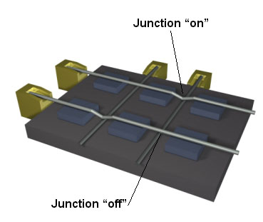
Central to all modern computers is Random Access Memory (RAM), where computer instructions and data are temporarily stored while the computer is running (RAM is erased when the computer is turned off, so that the only permanent copies of data are on the hard drive, which is much slower than RAM). A new RAM architecture, based on carbon nanotubes, has been proposed. In addition to delivering much higher bit storage densities (due to the small size of nanotubes: on the order of 0.5 to 4nm), these offer the possibility of storing data in a nonvolatile way. That is, while normal RAM is erased when the power is turned off (since it stores data in electrical signals), nanotube RAM would retain data without power (since it stores data as physical, mechanical deformations). This not only offers the possibility to do without hard-drives, but makes RAM more energy efficient (since power is not used refreshing data storage locations that are not accessed often). The architecture involves a two-dimensional crossed array of nanotubes (alternately, only one of the dimensions need be nanotube-based, as long as the other dimension has the necessary resolution and electrical properties). Using a bias voltage, a mechanical 'kink' can be introduced into a nanotube at a desired location. This kink greatly changes the electrical resistance of that junction, which is an easily measured property. The kinking process is fully reversible, allowing data to be written, erased, and rewritten at will. Moreover, switching speeds into the gigahertz range (faster than modern RAMs) appear possible. The architecture is amazingly simple, making it plausible for use in actual devices. Of course, nothing more than a four-bit prototype storage device has been produced so far.(1) Also, many challenges remain, such as the efficient production of the exact type of nanotubes required (and of the proper length), and convenient industry-scale wiring of the devices (the prototype was painstakingly wired by hand). Nevertheless, the advance in computer speed which could be realized if slow and cumbersome hard drives could be eliminated in favor of fast and vast RAM arrays is enticing. One of the major bottlenecks in modern computer speeds is the slow access time of hard drives, as compared to RAM and CPU clock speeds (it is this which is responsible for long load times: the delay in a program actually running after it is started, whereas the fast RAM and CPU are responsible for the seemingly delay-less operation of the program thereafter).
|
|
| NANOTUBE TRANSISTORS | |
|
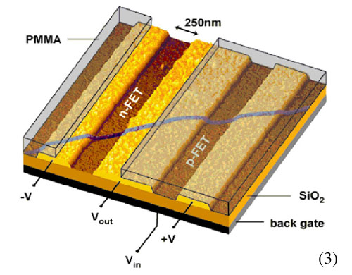
Nanotubes have also been used to generate transistors which operate very similarly to conventional Field Effect Transistors (FETs). Researchers were able to generate n-type and p-type regions both by conventional phosphorous implantation (after masking steps), or by thermal oxidation.(2) The transistor operated properly, with high switching speed and acceptable gain (meaning it could be used to drive another transistor as part of an integrated circuit). Although the small size of the nanotube means that the transistor itself could be made very small (a few nm wide, by tens of NM long), the early prototype had comparatively large contact electrodes, making the device fairly large. As before, the challenge for further development is to somehow generate the proper types of nanotubes, and to anchor them at predefined locations in a way that is amenable to large-scale production. Nevertheless, this demonstrates that nanotubes can operate like transistors. It should also be pointed out that nanotubes have the advantage of being to act as both wires and electronic devices. Since the transistor is built into a specific section of the nanotube, it is automatically wired up. Networks of transistors can be made by building them along nanotubes, with appropriate cross-connects.
|
|
| NANOTUBE ELECTRONICS | |
|
The above examples suggest that carbon nanotubes could be used to make electronic devices. Since nanotubes can function as wires, transistors, and nonvolatile memory elements, this suggests the possibility of highly micronized and integrated circuit design. Simple logic elements, such as NOR gates and NOT gates (inverters) have been produced using carbon nanotubes.(4) With these building blocks, essentially any computer chip design can now be realized, at least in principle. Other research groups have also shown that crossed nanotubes can be welded together, by exposure to an electron beam in the presence of carbon impurities, thus allowing for separate nanotubes to be linked together.(5) High energy can cut a nanotube. Thus, nearly all the elements for wiring together complicated circuits appear to be in place. Only time will tell if nanotubes will indeed be used for electronics.
|
|
| REFERENCES | |
|
|
|
|
|