Nanotechnology:
A Brief Overview
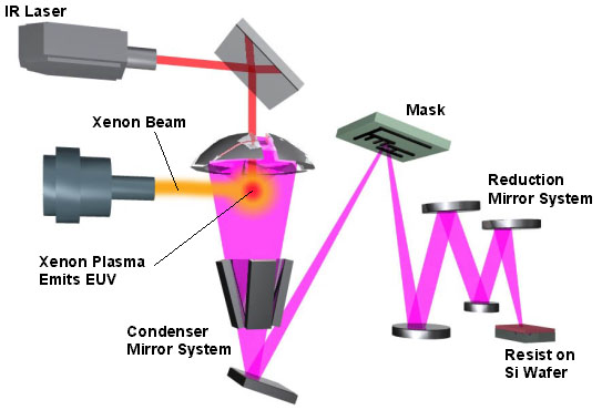
| EXTREME ULTRAVIOLET LITHOGRAPHY | |
|
In order to meet the demands of next-generation microprocessors, the industry has begun investing in Extreme-Ultraviolet Lithography (EUV). Compared to optical lithography, this system is much more complicated. To obtain radiation in the EUV (specifically at 13.4nm), a stream of xenon gas must be excited with an IR laser. Since there are no known substances that are transparent at 13.4nm, lenses cannot be constructed. Instead, the entire optical system must be built out of mirrors. Moreover, conventional mirrors won't work. Instead, mirrors made by multilayered stacks of materials with contrasting dielectric constant are used (typically alternating molybdenum and silicon or beryllium). These mirrors will reflect light, via constructive interference, whose wavelength exactly matches the spacing between the layers. Producing these mirrors (especially with spacings of ~13nm) is very costly. Luckily, a 4X reduction system, as with optical lithography, is possible, meaning that mask tolerances need not be much better than in current systems.
|
|
| ELECTRON-BEAM LITHOGRAPHY | |
|
Another possible way to push beyond the realm of optical lithography is to take a hint from TEM/SEM: if light is too large, use electrons. Indeed e-beam lithography has been used for many years to define surface features below the limits of optical techniques, using magnetic lenses to direct electrons onto a surface. It is useful, for instance, in producing masks with high feature fidelity. The spot size of an e-beam can be very small (0.5nm), but the system is limited by the scattering distance of electrons upon hitting the resist. Sub-100nm features are routinely produced using this technique. The main problem, however, is that it is a serial process. To write an entire chip using a scanning electron beam would take hours, which is a far cry from the minutes of exposure that mask-based systems use. This has prevented the widespread implementation of e-beam systems. Projection systems based on scattering masks are being developed. Essentially, a scattering mask is placed between two projection systems with an aperture. The mask is a thin layer of SiN with Cr or W features, which strongly scatter electrons. Electrons only escape if they were not scattered, allowing surface patterns to be defined. This system, however, has many problems. Since electrons carry considerable energy, the mask and wafer tend to heat, causing them to become distorted, which destroys the nanometre resolution required. Using low energy electrons solves this problem, but slows the exposure process, making it almost as slow as serial writing.
|
|
| ION BEAM LITHOGRAPHY | |
|
Instead of using electrons, one can imagine using ionized atoms instead. Since ions are much heavier than electrons, it is more convenient to control them using electrostatic lenses. Small spot sizes are possible for ion beams (~6nm), and heavy ions don't scatter nearly as much as electrons do. Unfortunately, using an ion beam is a serial process, and inherently slow. Moreover, to prevent damage to samples, lower energies must be used, which makes writing even slower. A stencil mask system has been proposed, with reduction of the image using electrostatic lenses, but this complicates writing considerably. Many features are difficult to define using stencil masks, and require two or three exposures to achieve the same features which can be obtained in one exposure of a transmission mask. Nevertheless, ion beam systems have been shown to create extremely small features, with high aspect ratios (for example, lines 8nm wide but 50nm deep).
|
|
| X-RAY BEAM LITHOGRAPHY | |
|
One might ask: "Why not simply use even shorter wavelengths of light?" Using radiation past EUV is difficult, but possible. (It is interesting to note that EUV was originally called 'soft X-rays,' but the name had to be changed so as to not scare off investors. X-ray techniques have always been very expensive.) X-rays are the highest-energy light we can imagine using (gamma rays would be far too energetic, and are too difficult to produce). X-ray radiation is very difficult to obtain, requiring a synchrotron or laser-induced plasma for a high-quality beam, but wavelengths on the order of 0.5 to 4nm are possible. There is, however, no projection system possible. Although X-rays can be manipulated using, for example, crystal surfaces (which will constructively interfere to reflect a beam of X-rays), creating a full projection system based on this principle would be very difficult. Thus, the only remaining possibility is a shadow mask, without any image reduction (the mask is usually 2microns of silicon carbide, with Au, W, or Ta absorber features). Thus, a mask is placed near the sample (~10microns), irradiated with X-rays, and an exposure pattern develops. This means that the mask itself must have the same feature sizes as what is being created, making mask creation much more expensive. The technique is limited by diffusion of photo-electrons, and is still diffraction-limited. To reduce diffusion, lower energy radiation can be used, but this increases the diffraction (and reducing diffraction increases diffusion). Sub 30-nm features can be produced with remarkably high aspect ratios (>10:1).
|
|
| PROBLEMS | |
|
The above techniques all use much higher energy radiation in order to circumvent the wavelength limitations of light. This introduces many problems, however. First, the sources and optical systems become much more expensive. Second, the production of the mask master becomes more expensive (as we define smaller and smaller features, the mask fidelity becomes more and more crucial). Third, the high energy radiation means that mask damage will occur much faster, so that masks cannot be used for as long as in traditional techniques (which greatly increases operating costs). Lastly, mask alignment becomes very very crucial if we ever intend to build real devices. Even if you are able to define 4nm features, this is useless if subsequent exposure steps are not aligned to within this same 4nm. Mask alignment is a big problem in the industry, with no simple solution. How can we do better? Many tricks have been suggested. For instance, the near-field (evanescent) component of light contains high spatial frequencies which circumvent diffraction limitations. Thus, a mask in intimate contact with the substrate could beat the diffraction limit. Cleanliness tolerances, however, become crucial, since even the smallest impurity could cause the mask to be raised above the substrate. Conformable masks have been investigated but have their own problems. Lithography on elastic polymers, which can then be compressed to reduce feature sizes has been demonstrated, but suffers from material resolution limitations. Lithography based on using AFM tips to 'write' surface patterns has demonstrated ~15nm resolution. The process is inherently serial, but arrays of hundreds of tips have already been produced. Essentially, it appears that, although lithography is a very powerful tool, and will be pushed much further, it cannot rule at the nanoscale. Something else is needed.
|
|
| REFERENCES | |
|
|
|
|
|