Nanotechnology:
A Brief Overview
| OPTICAL LITHOGRAPHY | |
|
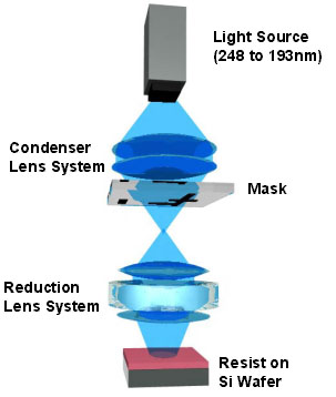
In the previous discussion of Moore's Law, it was concluded that new techniques would be needed to advance technology at the pace we are becoming accustomed to. But why? Why can the current techniques not be pushed harder and harder, making ever smaller devices? In the modern microelectronics industry, chips are made using optical lithography. Without getting into too many details, this involves long, complicated sequences of manufacturing steps. Some steps use optical lithography to define a surface pattern, and then steps involving chemistry are used to use this pattern as a template, or build additional material on top of preceding layers. |
|
 |
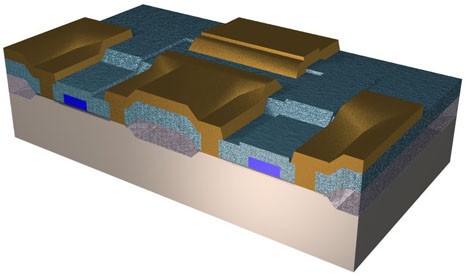
Below, a cross-sectional schematic of a crude CMOS inverter is shown. The layered nature of the device structure is evident. |
|
|
|
| DIFFRACTION LIMIT | |
|
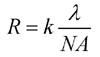
Since optical lithography works so well (producing 180nm features in modern Intel fabs), the question becomes: "Why not simply use masks with ever smaller features?" Obviously smaller mask features translates to smaller surface features. While this is true, there is another limitation to any optical system: the wavelength of light used. The resolution of any optical system (be it a microscopy or lithographic system) is limited both by configuration and the wavelength of light:
|
|
| Where the resolution R, is defined by configuration features (k is usually on the order of 1, and NA, the numerical aperture, on the order of 1.6), and the wavelength of light. This effect is called the diffraction limit. Diffraction is an inevitable consequence of the wave nature of light, and is responsible for the spreading of light as it passes through, for example, a slit cut into a screen. This means that feature sizes can typically only be made on the order of the wavelength of light used. At best, features at half the wavelength of light can be created, but no smaller. | 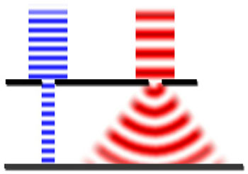 |
|
The question now becomes: "Why not just use shorter and shorter wavelengths of light?" The answer is: "That's exactly what is done." Unfortunately, this is not so easy. The industry used to use light sources like xenon lamps, using light of 450-350nm. With increasing demands, the industry switched to 248-193nm light. Now, the industry is switching to use Fluorine lasers, which emit at 157nm. As the wavelength is reduced, however, the situation becomes more and more complicated, and more expensive. The sources become more costly to produce, and lenses transparent at the given wavelength become harder to find.
|
|
|
|
|