Nanotechnology:
A Brief Overview
| SEEING THE NANOSCOPIC | |
|
To begin, it is worth discussing how researchers can "see" things at the scale of the nanometre. I will discuss two classes of techniques that are used: scanning probe microscopy (AFM, STM, etc.) and electron-beam microscopies (TEM, SEM). There are many other useful techniques for probing at the nano-scale (such as near-field scanning optical microscopy, NSOM), but the following techniques will give a flavor of what can be done.
|
|
| ELECTRON MICROSCOPY | |
|
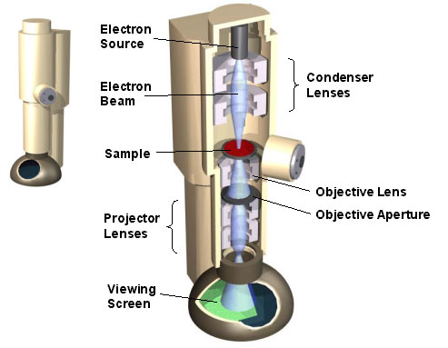
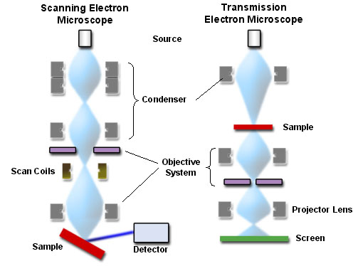
TEM (Transmission Electron Microscopy) allows the visualization of thin slices of material with nanometre resolution. Top of the line instruments have sub-nanometre resolution, and can almost resolve the electron density of individual atoms. A TEM operates much like a light microscope, but uses electrons instead of visible light, since the wavelength of electrons is much smaller than visible light (recall that the resolution limitation of any microscopy is based on the wavelength of the probe radiation). Since electrons are used instead of light, glass lenses are no longer suitable. Instead, a TEM uses magnetic lenses to deflect electrons. Beyond this, a TEM is very similar to a conventional microscope, complete with condenser lenses, objective lenses, and projector lenses.
Electrons are collimated from the source, passed through the sample, and the resulting pattern of electron transmission and absorption is magnified onto a viewing screen (the image is typically recorded with a CCD camera). The image which is generated is a 2D map of the material's density (which can be used to map topography in thin samples as well). In Scanning Electron Microscopy (SEM), the electron beam is not projected through the whole sample area. Instead, it is raster-scanned across the surface, and the secondary electrons, or x-rays, emit from the surface are recorded. This generates a lower-resolution image, but allows the direct mapping of surface features, and can even be used for elemental analysis (by study of the x-rays).
|
|
| SCANNING PROBE MICROSCOPY | |
|
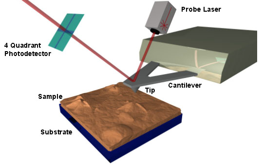
Scanning probe microscopy (SPM) involves running a nanometre-sized probe along a surface, and measuring its deflection. This allows the topography of the surface to be mapped out. Variations of the technique allow different aspects of the surface to be mapped out (such as density, viscoelastic response, magnetic behavior, density of electronic states, etc.). The simplest SPM technique is Atomic Force Microscopy (AFM).
The figure above is a highly schematic view of an AFM. Essentially, a micrometer-sized cantilever has an extremely sharp tip attached to it, which is sharpened to about 30-50nm at the end. A low-power probe laser beam is reflected off of the top of the cantilever, and into a four-quadrant photodetector, which records the position of the reflected beam. Note that the probe beam need not be perfectly aligned (as long as some of the beam is reflected into the detector, and the surface doesn't reflect too heavily into the detector), and need not even be smaller than the detector (since the difference between the quadrant signals allows the determination of the beam position). The photodetector measures the position of the reflected beam, which in turn gives information about the position of the cantilever, hence the tip. If the whole apparatus is raster-scanned across the surface (or the sample is scanned under the microscope), then an image of the surface-relief can be generated. Essentially, the continual deflections of the cantilever give information about the height of the surface at that point. A highly schematic video animation of this scanning is available (loop your video player if possible). Although the animation shows the photodetector recording the deflection of the cantilever as a function of position, real instruments are typically operated in a constant-deflection mode. In essence, the instrument records the vertical movement of the apparatus which was required in order to keep the deflection constant. This returns the same topography information as before, but gives the instrument a greater dynamic operating range. The example above uses a laser to measure the cantilever deflection, which is typical for AFM, although other sensory-feedback techniques can also be used. Many other SPM techniques exist. For instance, by functionalizing an AFM tip, the surface chemistry can be mapped. By measuring the twisting of the cantilever arm, friction can be mapped. By pressing the tip into the surface, density and viscosity can be measured. Another technique, Scanning Tunneling Microscopy (STM), uses the tunneling current between the tip and a conductive sample as a very sensitive probe of the tip-sample separation. This allows the mapping of surface topography down to the size of a single atom, and allows the visualization of the local density of states. There are many modes of operation of all the microscopes presented here. Interested readers should consult authoritative sources on the subject.
|
|
|
|
|